Hardware Considerations
Input/Output Delays
When synchronizing processing circuits users should be aware of delays associated with the I/O of their hardware devices. Users can synchronize I/O using delay components provided in RPvdsEx. See Delay Functions, for more information.
The table below provides a comparison of the delays associated with types of I/O and components.
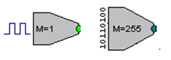
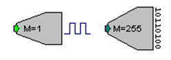
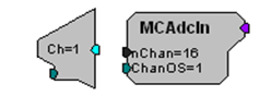
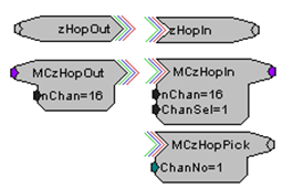
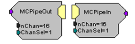
DAC and ADC Delays
Several of the System 3 processor modules use Sigma-Delta digital-to-analog and/or analog-to-digital converters. These converters provide over-sampling that generates signals up to 90% of the Nyquist frequency (half the sample rate) without the need for additional anti-imaging and anti-aliasing filters. While these devices provide for superior conversion quality and extended useful bandwidths, they have an inherent fixed group delay. When synchronizing the processing circuits with external devices via triggers, and so forth, one must account for associated delays in the converters being used.
Note
Information about delays and converter specifications, including amplifier related delays, can also be found in the technical reference for each device.
Sigma-Delta Sample Delays
The table below lists the devices that use Sigma-Delta converters along with their associated delays.
See Delay Functions, for a complete list of components that can be used to synchronize circuits when needed.
PCM Sample Delays
The table below lists the devices that use PCM converters along with their associated delays. PCM converters have a much shorter delay and, in general, do NOT necessitate the use of a delay component.
The Sample Clock and Sampling Rates
TDT's System 3 processors have a continuously running sample clock. The rate of this clock can be set to match the bandwidth of the signals you are working with. For example, studies with humans need a 20 kHz bandwidth, so the sample clock should be set to 50 kHz. At that rate, TDT devices that use sigma-delta type D/A's and A/D's can utilize nearly a 25 kHz bandwidth with no anti-aliasing filter.
Each TDT device has a fixed set of sample rate capabilities. The use of high performance sigma-delta DACs makes supporting completely arbitrary rates unreasonable in some devices. For example, the RX8 does not use sigma-delta DACs so it can offer any rate (derived from 25 MHz) while the RX6 uses sigma-delta DACs and thus supports a limited set of sample rates.
Note
The RX8 can be configured with sigma-delta converters and/or PCM converters. The realizable sampling rate depends on which type of converter is used. See the System 3 Manual for more information on selecting an appropriate sampling rate for your RX8.
The setup dialog in RPvdsEx will always return the true available rate for any device when the Check Realizable button is clicked.
Converting Sample Rates
Files recorded with other systems (including TDT System II devices) will have different sample rates. To convert files to System 3 requires changing the sample rate. Programs like Cool Edit allow you to change the sample rate of a signal. In addition MATLAB's Signal Processing Toolbox has resampling tools.
Sample Rate Synchronization Issues
Problems with synchronizing waveforms (such as a triangle wave) and with generating proper delays on two devices are typically a result of differing sample rates. The device with the higher rate can generate waveforms or delays with more resolution than the device at a lower rate.
Sample Rate Related Timing Issues
TDT software that offers arbitrary delays always bases the actual delay specified on the lowest sample rate used. If possible, use standard sample rates that will be related by a simple factor of two, four, etc. If you are using any of the non-linear generator components, be aware that only frequencies related to the sample rate by an integer multiple can be generated.
Component parameters that define a high, low, or delay period based on time are directly related to the sampling period. There is always a fixed difference between expected and actual values related to the sample period (inverse of the sample rate). The maximum possible difference with these components is ± the sample period.
When using these components, the actual time value will be the closest interval depending on the sample rate.
For example, at 100 kHz, a PulseTrain set to go high for 2 ms would be high for 1.9968 ms, because the sample period is 10.24 us.
Because these slight differences are less noticeable on devices using oversampling, such as those using sigma-delta converters, this issue is most noticeable when synchronizing several devices using different types of converters.
The table below shows the possible difference at different sample rates.
The actual length of time the component will remain high is the multiple of the sample period that is the closest to the set time.
For example, the table below assumes a component, such as a PulseTrain, is set high for 2 ms. The actual time the component would remain high and the expected difference are in the final two columns.
Cycle Usage
The main function of the DSP is to execute the processing chain; however, the DSP must also control or manage each aspect of the processor module. It must control the converters, move data, and pass instructions to and from the PC across the zBus/PC interface. On each tick of the sample clock the DSP:
- Executes the processing chain
- Performs "house-keeping" tasks
- Transfers data to and from the host computer across the zBus interface
Again, all of this must happen within one tick of the sample clock. You can imagine that as the sample clock gets faster, or the processing chain gets more complex, the DSP has less time to perform all of the necessary functions. At some point the DSP can no longer keep up, and errors occur. DSP/PC communication suffers and some components in the processing chain are no longer updated. i.e. when the amount of processing exceeds the sample period.
In fact, the window for communication with the host PC is entirely dependent on the time it takes to execute the processing chain. The DSP prioritizes the processing chain over PC data transfers. Thus, if executing the processing chain takes up 75% of a given sample cycle, the DSP has less than 25% of the remaining sample period to move data across the DSP/PC interface.
Cycle usage is a measure of the DSP workload including DSP housekeeping and processing chain execution. It is expressed as a percentage of the sample period consumed by these tasks. If cycle usage is near 100%, no data can be exchanged with the host PC. Furthermore, when the processing chain exceeds 100% cycle usage, the execution of the chain breaks down, and errors occur.
Each DSP has a set number of DSP cycles per tick of the sample clock. Cycle usage is dependent on the sample rate of the system, the processing power of the RP, and the components used. The lower the sample rate the more complex the circuit design can be. High sample rates (>50 kHz) will often limit what components can be used. Very high sample rates (200 kHz or more) may limit a circuit to only a few components. At higher sample rates, the number of available DSP cycles is lower and the overhead (running the D/A converters etc.) is greater. Use only the minimum necessary sample rate for your needs.
The table below shows the relationship between the sample rate and processing power and lists cycle usage and overhead for each sample rate for the RP2 processor.
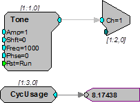
Many processors display cycle usage on a front panel LCD or VFD screen or using indicator lights. A CycUsage (cycle usage) component can also be added to a circuit to monitor how much processing power the circuit uses. When running a circuit from the RPvdsEx interface, connecting CycUsage to a ParWatch (parameter watch) helper component will display the cycle usage of the circuit.
The example below shows how to use a ParWatch to measure the number of cycles being used by the circuit that is running. In this example the Tone generator and DAC are using eight percent of the available cycles. Time slices may be used to reduce cycle usage by running calculations only on certain samples rather than on every tick of the sample clock.
Transferring Data between the Processor and PC
Most of the System 3 processors have onboard memory. Single processor devices with 32MB of memory can store eight million samples of uncompressed data and up to 32 million samples of compressed data. RPvdsEx has several built-in functions for using source data from the PC, such as DataTable and SourceFile. Users can also see the data by using ParWatch (parameter watch) and Graph. More sophisticated ways of transferring the data to and from the processor module require the use of ActiveX controls and some degree of programming.
USB Transfer Rates
USB transfers are limited to 100,000 samples per second of 32-bit data. Streaming signals to and from disks may be a problem for high sample rate or high channel number acquisition and presentation. For example, 16-channels of 25 KHz data produce 400,000 samples of data per second. Data reduction techniques, such as CompTo16 (Compress to 16) and ShufTo16 (Shuffle to 16), reduce the data size.
Gigabit Transfer Rates
Gigabit transfers are limited to 400,000 samples per second of 32-bit data. Signals can be streamed to/from disk without problem unless very high channel numbers are required. The Gigabit can stream a max of 16-channels of 32-bit data at 25 kHz. Data reduction techniques, such as CompTo16 (Compress to 16) and ShufTo16 (Shuffle to 16), can be used to reduce the data size.
Optibit Transfer Rates
The Optibit transfer rate is up to 8 times faster than the original Gigabit interface and also reduces the system's susceptibility to EMF. Devices are connected in a simple loop using provided high speed noise immune fiber optic cabling. Also, when using the Optibit interface, all devices (across all caddies) are automatically phase locked to a single clock. The Optibit interface supports high channel counts but is still subject to limitations. Data reduction techniques such as CompTo16 (Compress to 16) and ShufTo16 (Shuffle to 16) can be used to reduce the data size.
Interface Performance Comparison
The table below illustrates typical transfer rates for each System 3 interface:
Transfer rates are in MB/s. NS: Not supported