Circuit Design Basics
Creating and Running a Simple Circuit
Earlier sections of the user guide introduced the components, macros, and provided some information about how components are linked. The best way of putting all of these concepts together is to create and run a simple circuit. Follow the steps below to implement a simple counter circuit and become familiar with the basic mechanics of the circuit design process.
To create a simple circuit, follow the steps below:
Ensure at least one processor module is connected to your PC and turned on.
Launch RPvdsEx.
On the File menu, click New to open a new tabbed window.
On the Implement menu, click Device Setup .
In the Set Hardware Parameters dialog box, select your processor from the Type drop down menu.
The default index and sampling rate should be fine, so click OK to continue.
Double-click the tabbed window grid area to open up the Select component to place dialog box.
In the Select Category box, choose Counters/Logic .
In the Select Component box, click Counter .
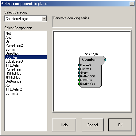
The Counter component implements a simple counting function based on the component's parameters. Using the default parameter values, it will count up from 0 to 1000 then reset and continue.
Click OK to add the component to the RPvdsEx workspace.
Double-click the tabbed window grid area again to open the Select component to place dialog box.
In the Select Category box, choose Helpers .
In the Select Component box, click ParWatch . This component displays the connected signal in RPvdsEx and is commonly used for debugging circuits.
To link the components, double-click the output port of the Counter component.
The cursor will change from a pointer to a circle with cross hairs. As you drag the cursor a line will appear.
Connect that line to the input port of the ParWatch by moving the cross hairs over the input port and clicking once.
A line and arrow will appear connecting the two components. This is called a link. The circuit should look like this:
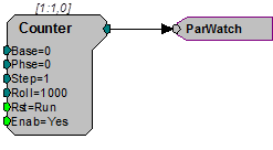
To run the circuit in RPvdsEx, click the  Compile, load, and run button on the Implement toolbar. This compiles the circuit, loads the circuit on the real-time processor device, and runs the circuit.
You should see the counter signal advance in the ParWatch component. The counter will continue until the circuit is stopped. Controlling the presentation of the signal requires additional components.
To stop the circuit, click the  Halt RP button on the Implement toolbar.
When the file is saved the circuit diagram and the control object are saved together. The resulting circuit file can be used with run-time applications.
Triggering
TDT's System 3 Processors support several triggering options. It is important to understand that the processor is always running a processing chain in normal operation. Therefore, instead of instructing the processor to 'play' the signal, you would instead trigger a gate to control the circuit output.
Triggering Options
The external, zBus, and software triggers are added to a circuit by adding a TrgIn component (see TrgIn).
External Trigger
Many of the System 3 processor modules provide an external trigger input that can be triggered by a TTL pulse from an external device. This TRIG input is separate from other digital input lines (typically found on 25-pin connector inputs).
zBus Triggers
zBus triggers are triggered from software. They are a convenient way to simultaneously trigger all zBus modules. TDT processors support two zBus triggers, A and B. They can be set as a pulse, always high or always low. The zBus triggers can be fired from RPvdsEx or from programs such as OpenEx, BrainWare, PsychRP or ActiveX controls.
Software Triggers
Software triggers are triggered from software, either by clicking the trigger on the Trigger menu in RPvdsEx or by issuing a software command that causes the trigger to fire. SoftTrg is initiated in a single circuit. The processors respond to ten unique software triggers. Software triggers do not allow precise timing across several modules because of the delay in sending and receiving information across the PC interface connection.
Digital Inputs
The RX processors have up to 40 bits of programmable digital I/O. See the technical specifications for each device for more information. The RP processors have eight digital inputs on the 25-pin connector. The RM has four or eight digital inputs on the 9-pin connector. These can be used in a circuit using the BitIn (BitIn) or WordIn (WordIn) components.
One Shot
The OneShot (OneShot) delivers one TTL signal when the circuit is run on the processor.
Pulse Train
The PulseTrain (PulseTrain) generates a train of TTL pulses with a specified pulse duration and inter-pulse interval. It is useful for repeating a stimulus that is triggered by one external trigger.
Gating a Signal
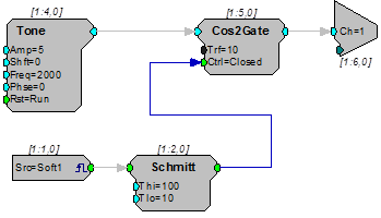
Gating functions gate the amplitude of the signal on and off with a set rise/fall time (msec). The rise/fall time is a static parameter and cannot be modified in a circuit. The gate begins to open when a trigger goes high (=1) and starts to close when the trigger goes low (=0). A Schmitt trigger can also be used to control the duration of the signal between opening and closing the gate. Triggering a Schmitt component sends a pulse out for a set duration. In this example the Schmitt trigger sends a 100 millisecond pulse to the Cos2Gate when it receives a software trigger (TrgIn). Triggers are one way users can control components in the processing chain. The Cos2Gate opens to 90% of the amplitude of the signal in 10 milliseconds and then starts to close at the end of the Schmitt pulse.
Acquiring and Storing the Signal
RPvdsEx uses memory buffers to store signal data for stimulus presentation and data acquisition.
Memory Buffers: Serial and Ram Buffers
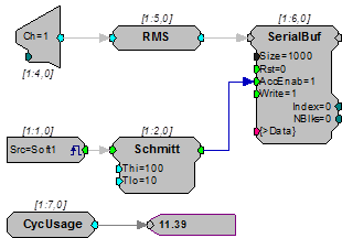
There are two types of buffer components, random access and serial. The random access component allows users to directly access any value in the buffer; however, the user has to tell the memory buffer where the data should be or is stored. The serial buffer automatically increments to the next position while it is acquiring or presenting signals.
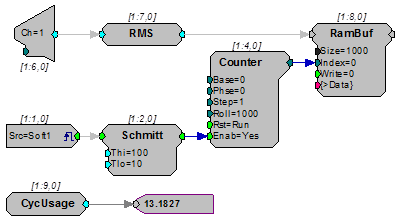
The examples below show how a random access buffer and serial buffer differ. In these examples the buffers acquire 100 milliseconds of signal. In the serial buffer example the data is saved as long as the Schmitt trigger that is connected to the AccEnab line remains high. In the RamBuffer example the Schmitt trigger must first start a counter to increment the Index on the RamBuf to the next position. Note that the cycle usage for the serial buffer is smaller.
Serial Buffer
Ram Buffer
Block Access
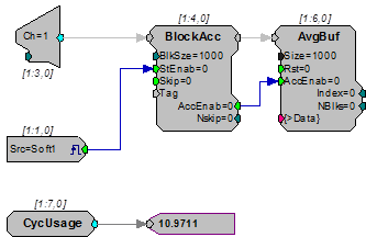
A BlockAcc (block access) component acquires a set number of signal values and stores them in a serial buffer. The advantage of a BlockAcc is that it automatically transfers a set number of points to the buffer. This is advantageous if the signal is to be averaged. In the example below a BlockAcc and an AvgBuf (average buffer) are used together to acquire a small signal.
The BlockAcc takes the place of the Schmitt Trigger in the example above. When the block access is triggered it acquires a set number of samples (1000) and then sends them out to a buffer. The example below demonstrates an averaged buffer. The average buffer, unlike the serial buffer, adds the incoming signals to the values in the buffer. A serial buffer or ram buffer would overwrite the old values with the new values.
The Data Port
All buffers and components that buffer signals, such as filters, have a data port. This port allows direct access to the memory location. Several components can access the data port to store, display, or download signals to the PC.
To learn more about using these components with the data port, see Data Port Access.
Signal Processing
Signals, whether acquired or generated, can also be filtered, smoothed, and analyzed for particular patterns. Two common signal processing techniques, filtering and signal splitting are illustrated below.
Filtering Gaussian Noise
The GaussNoise (Gaussian noise generator) produces unfiltered broadband noise. Filter and coefficient generating components can be added to the circuit to produce a narrow band of noise. In the example below, a Gaussian signal is bandpass filtered using a Biquad filter component. A ButCoef1 (Butterworth coefficient generator) generates the values for the necessary biquad filters. Biquad filters are used because of their stability. Filter properties can be changed in real time.
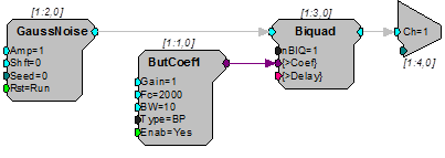
A single Biquad component filters the Gaussian noise. The ButCoef1 generates coefficients for a bandpass filter centered around 2000 Hz with a BW of 10 Hz. This bandwidth puts the 3dB corners at 2005 Hz and 1995 Hz. The output of the Biquad is then played out of DAC channel 1.
Note
The filter generated is rather broad. If a narrow band is required, filters can be connected together to narrow the bandwidth or users can generate their own filter values for use with our IIR and FIR filters.
To alter the values on the fly connect a parameter tag or Data Table to the Fc and BW of the ButCoef1.
Signal Detector: Splitting the Signal Path
The System 3 processors allow users to process signals in real-time without any modification from the PC. This allows users to detect changes in signal levels and respond in less than a millisecond. In the example below the circuit detects changes in an incoming signal and lights one of the outputs on an RP (RP2, RA16, or RL2) module.
In the example below a signal is filtered so that only signals in a particular frequency are detected.
Bandpass filter the incoming signal.
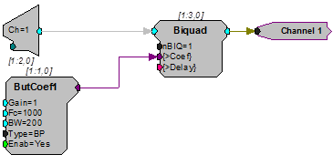
Detect signals that are at least five times greater than the background RMS level.
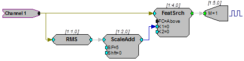
A Hop (Channel 1) is used to simplify the logic of the circuit. The hop allows the circuit design to be split. The hop does not alter the processing chain it allows the chain to be easier to follow and debug. A single HopOut can have multiple HopIns that split the signal.
The split signal goes to two components: the RMS (root mean square) and the FeatSrch (feature search). When the RMS is calculated it determines the criteria necessary to activate the FeatSrch. While a signal meets the criteria of the FeatSrch a logical value is set high (goes from 0 to 1). In this case the Signal must be 5 times the normal noise of the filtered signal for a pulse to be generated. All these parameters can be easily modified. The logical pulse can be used to light an output or to start acquisition of the signal or both.
In addition, delays can be added to the circuit so that the acquisition of a signal includes all of the waveform.
Scale and Add
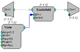
This circuit implements a simple AM modulator. The signal connected to the channel one A/D input will be 50% modulated by a 50 Hz sinusoid generated by the Tone component. The result is played from channel one of the DAC.
Note
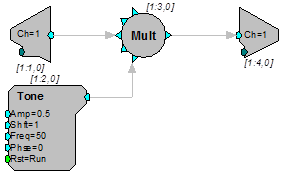
The circuit using ScaleAdd will run in fewer cycles than the alternate construct shown below using Mult.
Using Parameter Tags for Software Control
When your circuit is saved as a circuit file it can be used by all TDT application software and can be incorporated into custom programs you develop using a programming language that supports ActiveX.
Parameter tags are pointers that create named access points within your circuit. They can be used to control parameters and access data while the process chain is running.
The example below acquires, filters, and stores a multi-channel signal. The HPFreq and LPFreq parameter tags allow users to control the corner frequency of the cascaded filters while the dWav parameter tag allows the user to access the stored data for data visualization and analysis.
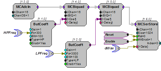
There are two ParTag components, a right and a left version, allowing you to choose the tag that will make your circuit easier to read. There is no functional difference between the two.
Parameter tags can be connected to any parameter input or any output. However, they cannot be connected directly to a signal input. To use a parameter tag with a signal input you must first route the signal path through a ConstF, ConstL, or ConstI component.