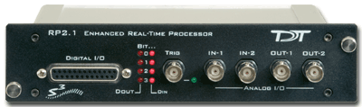
RP2.1 Real-Time Processor
RP2.1 Overview
The RP2.1 real-time processors consist of an Analog Devices Sharc floating point DSP with surrounding analog and digital interface circuits to yield a powerful programmable signal-processing device capable of handling a variety of tasks.
Power and Communication
The RP2.1 mounts in a System 3 zBus Powered Device Chassis (ZB1PS) and communicates with the PC using any of the zBus PC interfaces. The ZB1PS is UL compliant, see the ZB1PS Operations Manual for power and safety information.
Software Control
Software control is implemented with circuit files developed using TDT's RP Visual Design Studio (RPvdsEx). Circuits are loaded to the processor through TDT run-time applications or custom applications. This manual includes device specific information needed during circuit design. For circuit design techniques and a complete reference of the RPvdsEx circuit components, see the RPvdsEx Manual.
Features
Memory
The RP2.1 comes with 32 MB of memory for data storage and retrieval.
Digital Input/Output Bits
The digital I/O circuits include eight bits of digital input and eight bits of digital output that are accessed on the 25 pin connector on the front of the RP2.1. The bits of these ports can be programmed individually or as a 'digital word' and used in a variety of ways within the RP2.1 processing circuit, including implementing triggers, timing trigger responses, and lighting LEDs. The first four bits of the digital inputs and digital outputs as well as the Trigger/Enable input are mapped to LED indicators on the front panel of the RP2. There is an additional TRIG input BNC on the front panel.
D/A and A/D
The RP2.1 is equipped with two channels of 24-bit, 200 kHz sigma-delta D/A and two channels of 24-bit, 200 kHz sigma-delta A/D. Sigma-Delta converters provide superior conversion quality and extended useful bandwidths, at the cost of an inherent fixed group delay. See RP2.1 Technical Specifications for the group delay of each device.
Hardware
The 32 MB of SDRAM are used for storage of long stimulus waveforms and acquired data. All of the RPvdsEx buffer components, used to build circuits for the RP2, utilize the SDRAM memory. The RP2.1 communicates with and is programmed through the zBus.
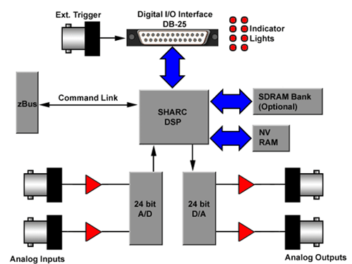
The RP2.1 is interfaced to the analog world via a two channel 24-bit analog to digital converter and a two channel 24-bit digital to analog converter. The RP2 system's I/O buffer handles ±10 V signals with excellent signal to noise performance. The RP2 contains a 100 kHz (50 kHz BW) A/D and a 200 kHz (100 kHz BW) D/A, while the RP2-5 has a 50 kHz (25 kHz BW) A/D and D/A. Both devices allow for user programmable sampling rates from the specified maximum down to 6.25 kHz. A special calibration program is used to calibrate the RP2's analog I/O offering very small gain and DC offset errors.
RP2.1 Technical Specifications
DB25 Connector Pin Out
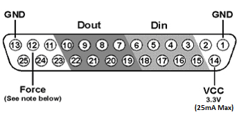
Note
TDT recommends the PP16 Patch Panel for accessing digital I/O.
Important
Force is used to reset the RP2.1, including deleting the device's microcode. It has no function in data acquisition or manipulation.
To reset the device:
-
Connect a wire (or paper clip) from pin 12 to pin 13 on the Digital I/O port.
-
Use the desktop short cut to run zBusMon.
-
With pins 12 and 13 shorted, click the 'Reboot System!' button. The RP2.1 will appear as a 'G21' device.
-
Right-click on the G21 and select 'Program G21'.
-
In the System3 Device Programmer window, click the Browse button next to the uCode File field and select RP21.dxe.
-
Remove the short from pins 12 and 13, and click the 'Program Device!' button. Do not use your computer until the device reprogramming is complete (approximately four minutes).